
TEL
021-59241040
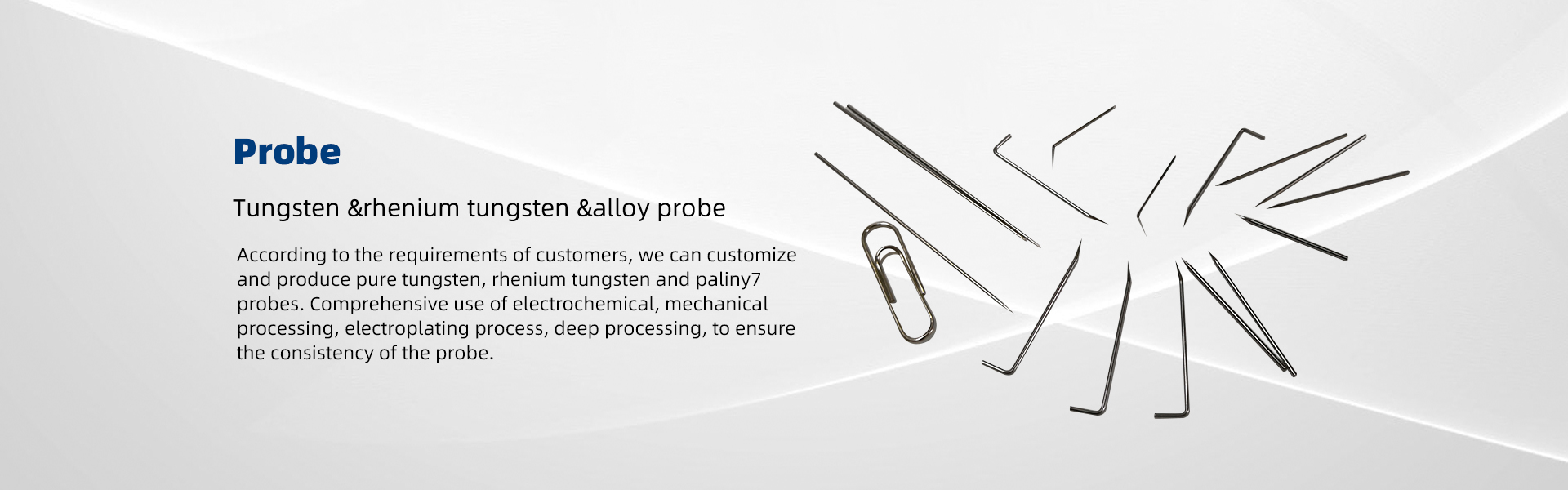
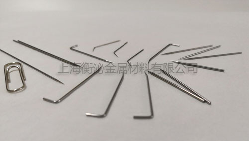 Tungsten probe
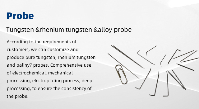
Our pure tungsten probe, rhenium tungsten probe and paliney 7 alloy probe are mainly used in IC, led, LCD and other chip detection, wafer detection and other industries. Suitable for all kinds of pad surface.
Adopts stable quality raw materials, and can provide domestic or Japanese tungsten materials according to various requirements of different customers, including pure tungsten (99.95-99.98%), rhenium tungsten and other raw materials. Tungsten probe has the characteristics of high hardness, high elastic modulus and so on. Alloy probe has been widely used in the field of LED chip detection. Its conductivity, modulus of elasticity, durability, optical output, reliability and mechanical stability can meet the customized requirements of customers.

We use electrochemistry, machining, electroplating technology, deep processing to ensure the consistency of probes. According to the requirements, we can customize the shape of the tip, including sharp tip, platform and arc. Our tip range is from micrometer to nanometer. The radius of curvature of the tip min can be controlled to 50nm. Before packaging, 100% of the needles are tested one by one.


Probe solutions:
The machining accuracy of hengmi is controlled at 0.001mm, and probes in different application fields can be customized according to the customer's requirements. In the aspect of tip processing, bending molding, slotting and other deep processing, the minimum control of the tip is 0.05um (50nm), the taper finish is below ra0.25 (almost mirror), and the uniform can also be determined according to the customer's requirements, such as overall or partial nickel plating, tin, gold, die-casting copper sleeve and stainless steel sleeve Business.
Probe specifications and performance parameters